The Tandem bridge is ubiquitous. It appears in transmitters, tuners and similar apparatus. The useful frequency range is from a few kHz to 50 MHz or more depending on the transformer cores chosen.
This page is not concerned with the practicalities of building one. The internet contains hundreds of similar or identical designs. Instead, this page investigates the RF design equations and the limitations inherent in the circuit. For example, it is optimistic to call it a bridge. The equations for the reverse voltage shows that the bridge never achieves balance.
Some amateurs analyse the bridge by assigning volts per turn on each winding. This works fine and alleviates complexity but it fails to include the multifaceted behaviour of the device. This is demonstrated on other web pages and will not be repeated here.
Introduction
The Tandem bridge consists of only two components yet it is very complex and tedious to analyse. I have made the assumption that the two transformers are identical. However, there is no reason why this must be so.
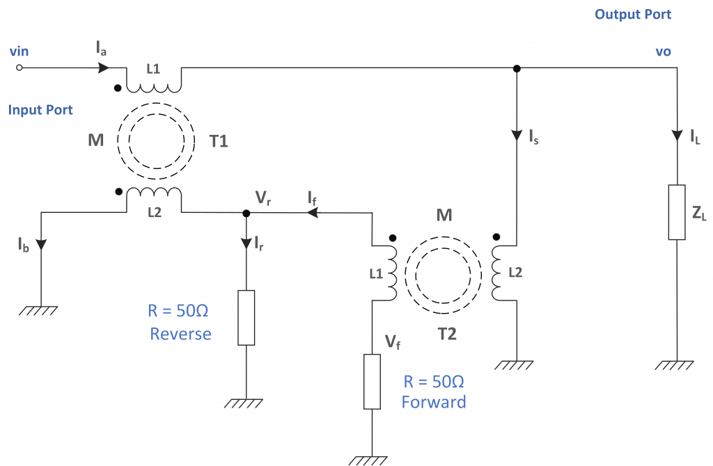
Figure 1 – The Basic Tandem Bridge
The tandem bridge is a compromise. The level of return loss depends upon on the winding inductance and the mutual coupling between them. At no time does the reverse voltage ‘Vr’ ever fall to zero even when the load is exactly 50 Ω. This circuit does not balance as such. Observation of the circuit suggests that this bridge must also introduce an impedance change in the transmission path. However, the tandem bridge is an excellent performer and deserves full analysis.
Key Equations
These four expressions define the performance of the Tandem bridge:
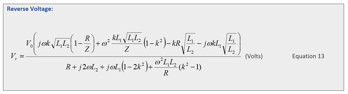
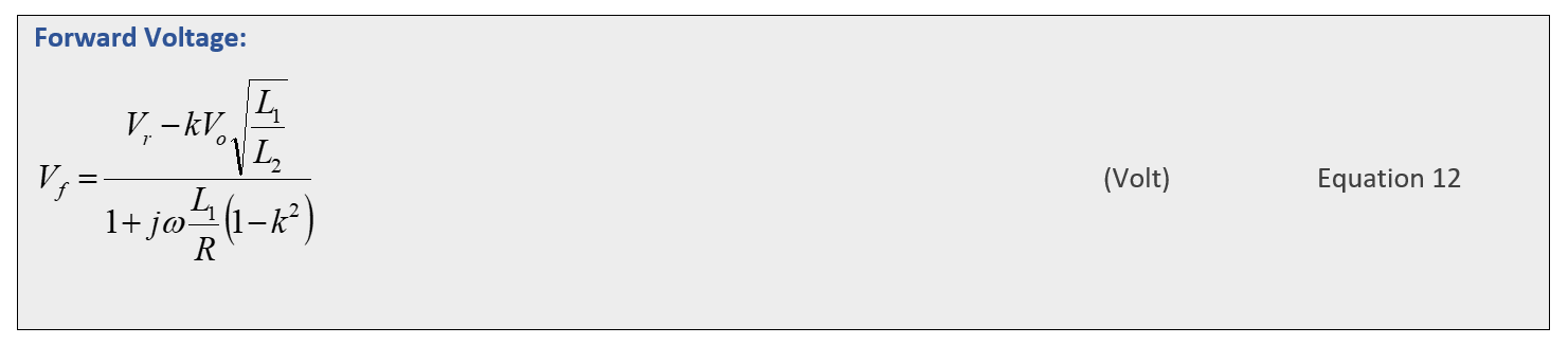
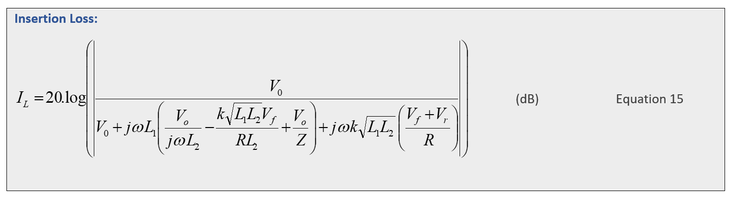
‘Appendix A’ of the attached document provides a derivation of equations 12, 13, 14 and 15 (if you are really keen). It is possible to further simplify these equations by replacing the inductor values with an expression involving the turns ratio N. However, the inductor values will change with frequency and are more fundamental than N.
Also avoided is expressing the complex terms in canonical form (a + jb). It is just not worth the time and effort bearing in mind that calculations of this complexity will, inevitably, be crunched by machine.
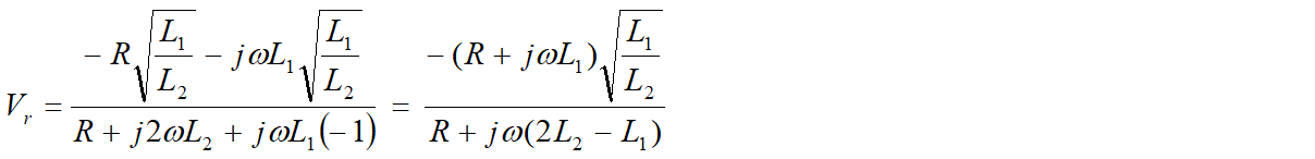
Minimum Reflected Signal
Equations 13 can be simplified by making assumptions. Assume that the coupling function k = 1, Vo=1 and the output impedance Z = R. Under these ‘balanced’ conditions equation 13 becomes:
As the frequency increases:
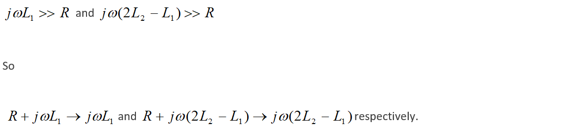
Hence, the minimum level is determined by the inductance values alone. Since the bridge must be practical with realistic inductance values, the minimum reflected level of the Tandem bridge is finite – the bridge never balances to zero. The following expression illustrates the limit.
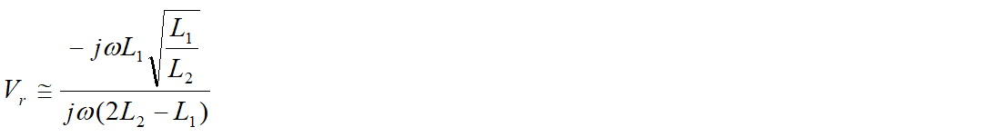
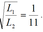
Assuming L2 >> L1 (In fact it is N x N larger where N is the turns ratio)

The negative sign indicates that the reflected signal is antiphase relative to the output signal. To be sure, I investigated an LTspice evaluation using ‘transient’ analysis and confirmed that both the forward and reverse signal appeared in antiphase compared to the output signal.
As an example, if a Tandem bridge employs cores with a turns ration N=11 and the inductance of a single turn on the ferrite core is L1 = 2.3 uH then L2 = 278.3 uH and so:

Forward Signal at Minimum Reflected Value
The forward voltage expression simplifies if k=1 and Vo=1. Also, if the reflected signal is low compared with the output voltage i.e. at -68.5 dB then:
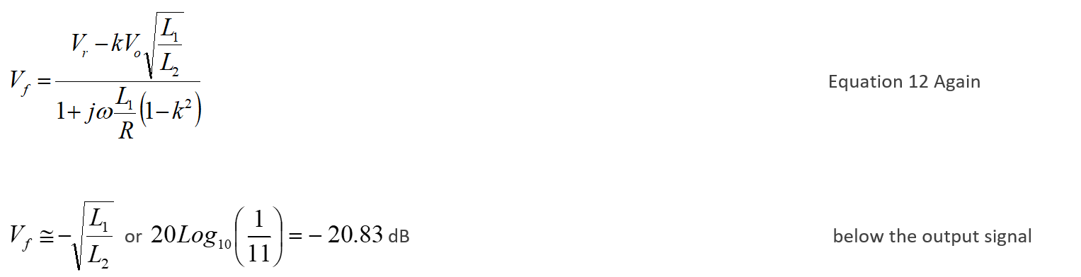
Hence, for N=11, the very best return loss is -47.67 dB.
Verification of Equation 12 and Equation 13
Equations 12 and 13 require verification. One way to do this is to test the results against validated circuit simulation software that calculates similar results using a different but equivalent approach. I employed LTspice which is very capable and free. Mutual inductance and k values define the coupling of inductors in LTspice in exactly the same way as in equations 12 and 13, enabling an exact comparison. LTspice, of course, calculates numerical values.
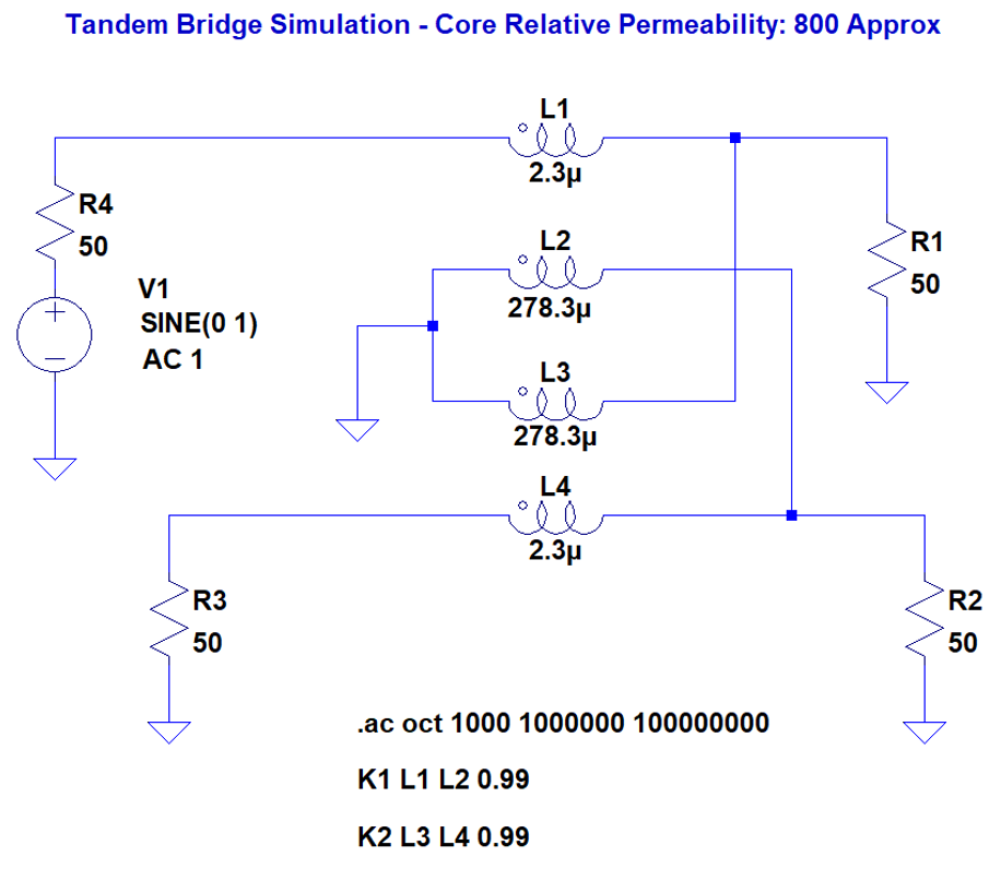
Figure 2 – LTspice Implementation of a Tandem Bridge
In the above LTspice example, if k=0.99, L1 =2.3 μH, L2 = 278.3 μH (N=11) and f = 2 MHz, then the forward, reverse and output signals calculated by LTspice are:
Output signal = – 6.057 dB (The output is effectively divided in half by R1 and R4)
Forward signal = – 26.936 dB
Reverse Signal = – 74.144 dB
Relative to the output signal (Add 6.057 dB to all three):
Output signal = 0 dB
Forward signal = – 20.879 dB
Reverse Signal = – 68.087 dB
Return Loss = – 47.208 dB
The calculation of equations 12 and 13 is best performed using capable mathematical software. The easiest and most universal way is probably Python or C. Any method will do as long as the complex numbers are properly implemented. It is best to avoid spreadsheets if you can.
For this document, I used ‘Mathcad’ which is a bit specialised but it provides a WYSIWYG representation. This is easier to follow than lines of ‘C’ code.
As an example:
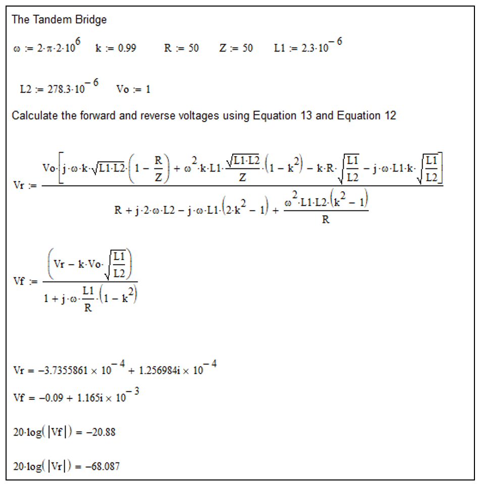
Figure 3 – Mathcad Evaluation – Verification
The above Mathcad sheet used the same parameters to calculate the forward and reflected voltages. Compared with LTspice, the results are correct to at least 2 decimal places. Similar calculations using different loads, different k values and different frequencies always gave comparable results. I conclude therefore that equations 12 and 13 are probably correct. (I say probably because these equations give steady state values and do not include transient terms that following immediate activation of the circuit).
Tandem Bridge – Return Loss – Verification
Does the Tandem bridge provide an accurate rendition of return loss? For a transmission system with an arbitrary termination, the reflection coefficient at an impedance discontinuity is described as:


Using k=0.99, L1 =2.3 μH, L2 = 278.3 μH (N=11) and f = 2 MHz as an example. The return loss for a range of Z (the load) can be plotted. The following Mathcad sheet does this for a range of Z real values from 0 to 200 Ω. Complex imaginary values for Z can be added – in this example it is set to + j1. Figure 4 shows the results for a near resistive load.
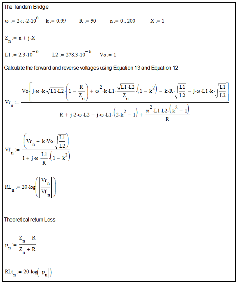
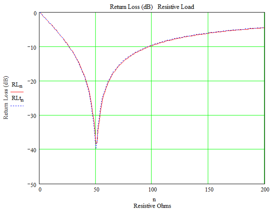
Figure 4 – Mathcad Worksheet – Reactance of +j1Ω (Essentially Resistive Load)
Figure 4 shows the theoretical return losses and the values returned by the Tandem bridge. They appear very close. The reactive part of the load impedance ‘Z’ was set to + j1 Ω for convenience to avoid divide by zero errors. However, the 1 Ω reactive component reduced the return loss from -47 dB at Z=50 Ω to -40dB at Z = 50 +j1 Ω! The bridge is very sensitive!
Figure 5 – Mathcad Worksheet – Reactance of +1Ω (Essentially Resistive load)
Figure 5 shows the theoretical and the Tandem bridge return loss for Z= (0 to 200) – j100Ω. Again, the two values are very close. I conclude that the Tandem bridge provides a good representation of the forward and reflected signals. This conclusion is intuitive – the signals at the forward and reflected port are just transformer-reduced constructs of the primary circuit.
Tandem Bridge – Input Impedance – Verification
Equation 14 calculates the input impedance of the bridge:
This is verified against an LTspice simulation. For example, using the same parameters as before: k=0.99, L1 =2.3 μH, L2 = 278.3 μH (N=11), Z=50 Ω and f = 1 to 50 MHz, the Mathcad sheet calculates the input impedance and plots it onto a graph against frequency.
Input impedance results from the LTspice simulation were taken manually at 2, 10, 20, 30, 40 and 50 MHz using the graph and status bar. These were plotted onto the same Mathcad graph and shown as blue circles.
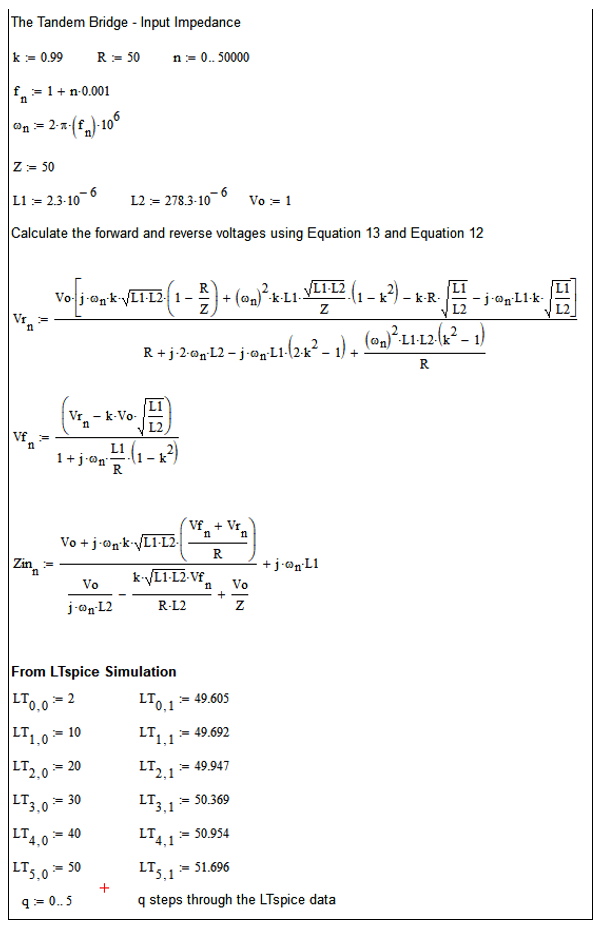
Figure 6 – Mathcad Calculation of Input Impedance
The results were identical to three decimal places or more. At low frequencies, the input impedance magnitude of the bridge is less than 50Ω probably due to the shunting effect of L2 across the output. At higher frequency, the series impedance of L1 starts to dominate.
The input impedance is easily converted into VSWR. For the condition stated, such a bridge would provide an insertion VSWR of less than 1.2 at frequencies below 30MHz. The data provided here is for verification only.
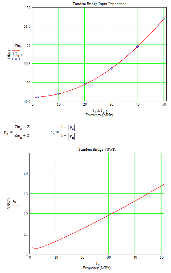
Figure 7 – Tandem Bridge – Input impedance and Input VSWR
Tandem Bridge – Insertion Loss – Verification
The insertion loss of the bridge can be calculated using Equation 15. This can be verified against an LTspice simulation. For example, using the same parameters as before: k=0.99, L1 =2.3 μH, L2 = 278.3 μH (N=11), Z=50 Ω and f = 1 to 50 MHz, the Mathcad sheet calculates the insertion loss and plots it onto a graph against frequency.
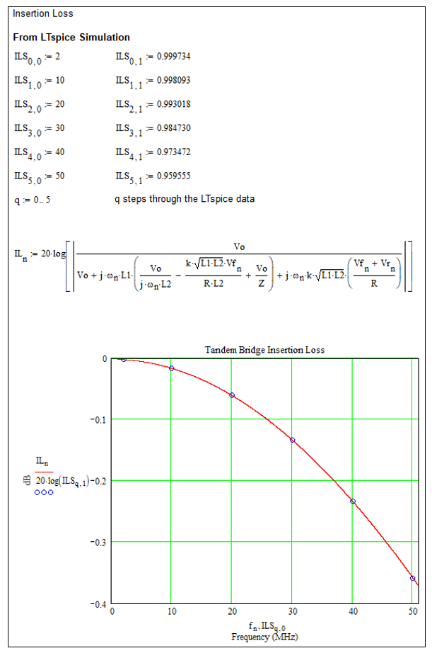
Figure 8 – Equation 15 and LTspice Provides Identical Results
The results are essentially identical. I conclude the four equations 12, 13, 14 and 15 provide an accurate mathematical description of a Tandem bridge. I should point out that assuming k=0.99 probably underestimates the performance of the transformers. This value was chosen at random just for the verification process.
Appendix A – Proof of the Equations
The outline proof of equations 12, 13, 14 and 15 is more tedious rather than difficult. I have to admit to making several attempts (about 10 attempts over several months) before getting the forward and reverse voltages correct. I suspect that no one will have any interest in the proof so I have included it in Appendix A of the enclosed PDF: Tandem Bridge Proof Only
The complete document is available here: Tandem Bridge Full
73 Chris