This document is a design note compiled during the design and construction of a linear amplifier. It is intended as a catalogue of ideas and thoughts to be shared. Some of the design ideas worked well, others failed miserably, but that is the nature of homebrew.
Warning
This is not a construction project. DO NOT BUILD THIS AMPLIFIER – I DO NOT RECOMMEND IT. If you really need or want a linear amplifier, then go out and buy a commercial product. It will work better, have residual value, look nice in the shack and it won’t kill you! This amplifier certainly will, given half a chance.
Design Notes
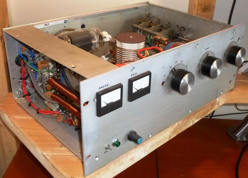
Figure 1 – Amplifier Front and side View – Panels Removed
The first version of this amplifier started service in the late 1970s and employed a pair of 813 tetrodes arranged in passive grid. That amplifier worked well but the power supply eventually failed making a mess. It was also dangerous (more dangerous than this one). The anode panel meter carried 3kV!
The amplifier and power unit ended up in the garage for 35 years. Unfortunately, I promised myself that I would complete the project when I retired. Over the years this became an obsession, and I found myself duty bound in 2018 to complete it. The plan was to complete the project, use it for a while, put it back in the garage, forget about it and then buy a nice ACOM 1500 or similar.
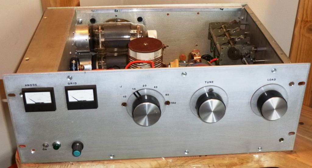
Figure 2 – Another View – Top Panel Removed
Circuit Diagram
The circuit diagram is very conventional and uninspiring.
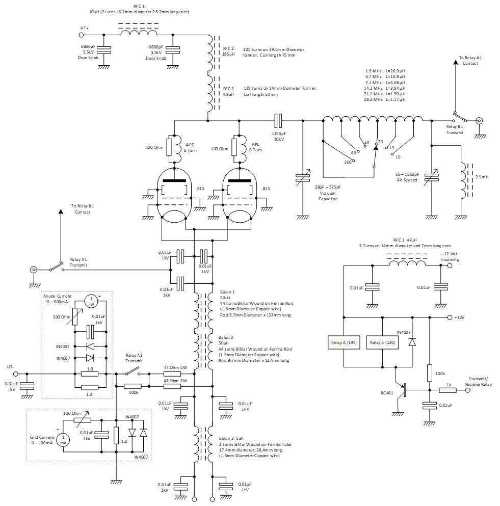
Figure 3 – Circuit of the Amplifier Compartment
The Power Supply
By changing the configuration to grounded grid, it is possible to eliminate the screen grid and bias supplies completely. The supply consists essentially of two very heavy transformers in a conventional arrangement.
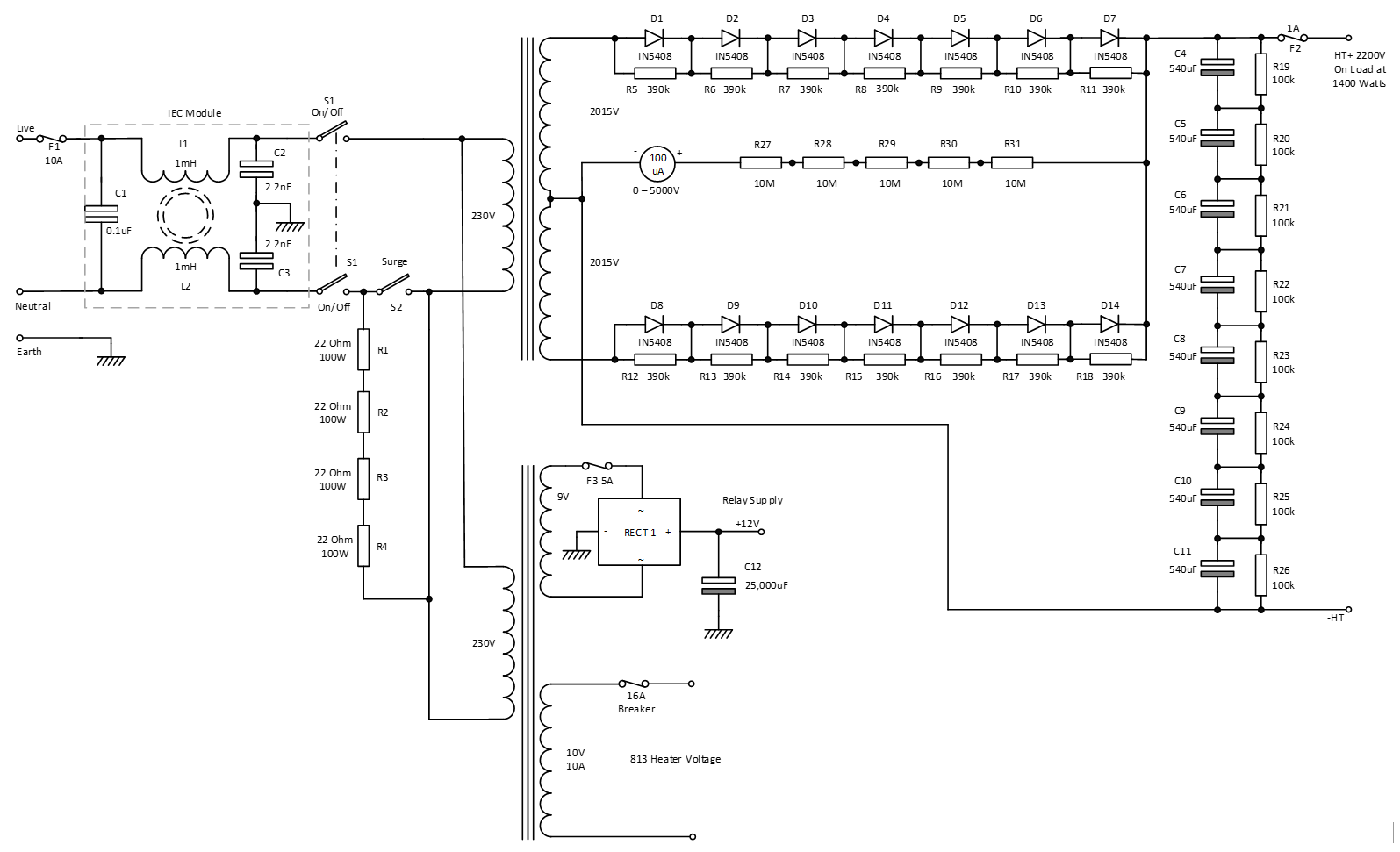
Figure 4 – The Power Supply Circuit
The hard part is finding a power transformer of sufficient voltage, sufficient power with useful taps. The assumed input power of the amplifier is 1400/1500 Watts and the target HT supply is around 2.2kV. Off load, this creeps up to around 2.5kV.
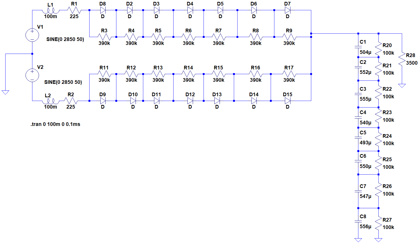
Figure 5 – LTspice Power Simulation
Figure 5 shows an LTspice simulation of the power supply using the measured values of the reservoir capacitors C1 to C8. Despite purchasing identical items from the same source, the measured values varied from 493 uF to 556 uF, which is within the specified tolerance. The equalisation resistors R20 to R27 (in Figure 5) help spread the HT voltage across each of the capacitors. However, differences still exist, for example, C8 measured 271 Volts whereas C1 measured 310 Volts. These values are well within the maximum rating of 450 Volts.
You may ask: Why bother simulating the power supply in LTspice? Well, the capacitors in the previous power supply exploded. I can’t be sure why but following the mayhem, the rectifier pack was found in a failed state probably due to over current, over voltage or just poor design. This time I wanted to be more careful and understand the peak and average current carried by the diodes.
The off-load voltage is 2.5 kV. Hence, C1 must be capable of supporting 341 Volts indefinitely. It is tempting to use only 7 capacitors with a theoretical maximum voltage of 3.15 kV. A better solution is to aim for a larger safety margin using 8 capacitors. Electrolytic capacitors make an awful mess when they blow! The resistors R20 to R27 each dissipate around 1.2 Watts. The resistors should be high voltage types.
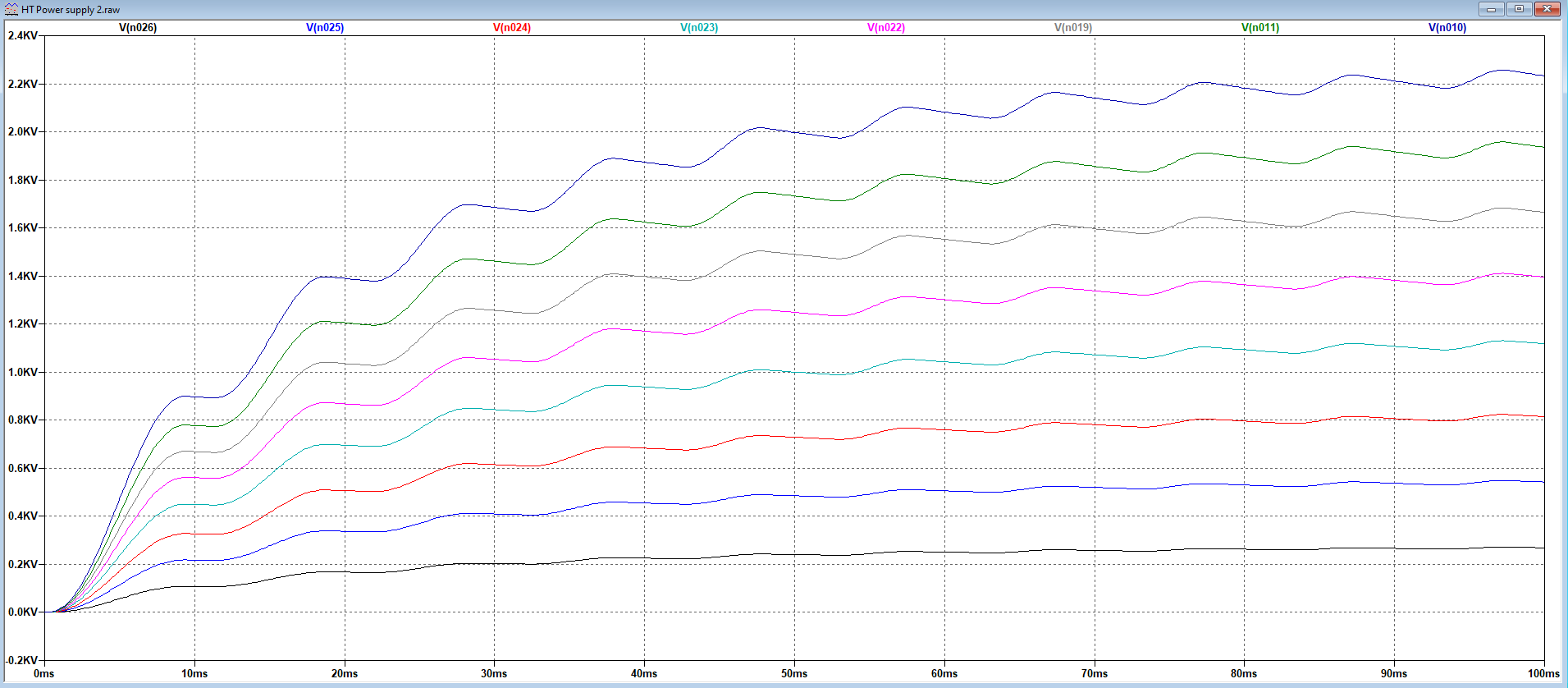
Figure 6 – Voltage on the Reservoir Capacitor Chain
Figure 6 shows the LTspice simulated voltage on each capacitor in the reservoir chain charging from cold (without the soft start). It takes 100ms to get up to full voltage with a 1500 Watts load. The diode pack consists of 7 x IN5408 power diodes in each leg. The peak inverse voltage rating is around 7kV and the average current rating is 3A.
LTspice tells me that the PIV applied to the diode pack is 5.2kV. At 1500 Watts, the diode transient current peaks to 2.4A over a short duty cycle and peaks to a maximum of 10.6A on the first charging cycle without the soft start. All this is well within the ratings of the diodes.
Construction – RF Chassis
The RF chassis consists of pieces of battered aluminium arranged to look as though they have purpose. I have to admit that chassis bashing is not my forte and some of the holes are superfluous! A perforated lid fits on the top with screws.
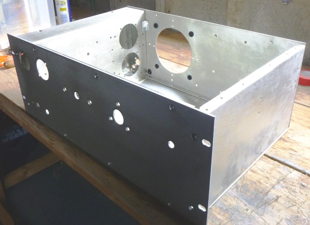
Figure 7 – Empty Chassis on the Bench
Being objective, the chassis is too large to house just the RF components but too small to house the power transformers. Failure to put in sufficient thought at the design stage, during the 1970s, resulted in limitations that still continue 50 years on! It is tempting to redesigning the whole project from the start. If I do that, I may as well put the money towards a nice new shiny ACOM.
Construction – Power Supply
The power supply is truly embarrassing. It consists essentially of two ridiculously heavy and overrated transformers, a bunch of rectifiers and a few electrolytic capacitors. I gave serious consideration to purchasing new modern toroidal units to reduce the weight.
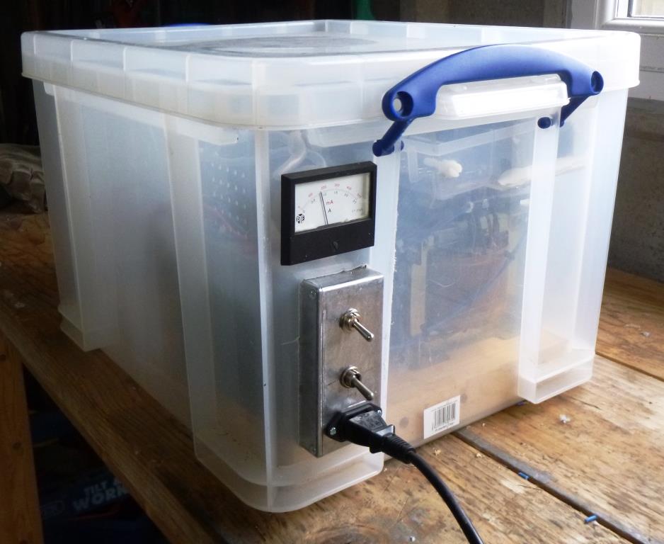
Figure 8 – Power Supply Input
A plastic container houses the power unit. In the UK, these are known as ‘A Very Useful Box’ and are available from a host of outlets. I would rename this one as ‘A Very Dangerous Box’ for obvious reasons. In normal use, I use a ratchet strap that passes around the outside of the box over the handles to prevent the lid from accidentally lifting.
An IEC lead and a filtered IEC socket provides 230V 50Hz input for the supply. Being house in a plastic box, the filtering probably serves limited purpose at HF. However, the filter does minimise the egress and ingress of conducted emissions at lower frequencies and is worth keeping. The volt meter originated from a PYE transmitter.
The IEC connector and the voltmeter provide additional safety features. Removing the IEC cable from the box and observing zero potential on the meter provides a level of confidence before fiddling inside the case. It is very easy to leave a permanently connected mains cable connected to the supply by mistake – I know I have done it on several occasions with other equipment!
The AC power wiring, resistors and switches all mount on a diecast box that pokes through the side of the plastic box. A pair of block connectors makes the wiring easy. The diecast box is safety earthed via the IEC lead. A thick core cable and wingnut arrangement provides an additional bond (in addition to the umbilical cord) between the PSU and the RF deck. This is ‘belt and braces’ I suppose, but it helps keep one out of the wooden box.
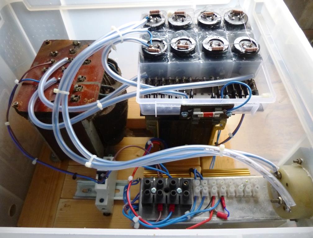
Figure 9 – Power Supply Unit Inside View (Partially finished)
A PVC component tray housed the eight 450V, 540 uF reservoir capacitors. Silicon sealant provided a simple but crude way of fixing the capacitors in place. The rectifiers and voltage divider resistors sit in another PVC tray mounted on a tag strip. Silicon fish tank tubing enclose all wiring carrying EHT to avoid voltage breakdown. Plastic nuts and bolts hold it all together.
Figure 9 does not show the umbilical cord – that emerges through a gland on the left-hand side of the box.
The circuit breaker (in the 10V heater circuit) turned out to be a useful feature. During long-term EHT breakdown tests (This involves leaving the EHT on for hours at a time.) it was useful to be able to turn off the 813 valves by disconnecting the heater supply using the breaker.
This breakdown testing also revealed another dangerous feature that I missed during the design stage. The EHT time constant is excessive. It takes a long time for the DC levels to fall to safe values following removal of the AC supply.
I deliberately chose large capacitor values to hold up the EHT during SSB peaks but eight 540 uF capacitors in series give 105 uF @ 2.5kV. The resulting no-load time constant is around 54 seconds. That is a long time to wait. At full charge, the capacitors hold around 328 Joules of energy. 1 joule is enough to kill!
Basic Specification
The basic specifications for this re-build are simple enough:
1. 160m – 10m. No WARC band settings on the PI-tank – see text.
2. Avoid individual PI or L input filters if possible – See text.
3. 2 x 813 Valves – mandatory.
4. Silent cooling fan – mandatory.
5. Grounded Grid.
6. Anode and Grid current meters – no anode voltage on meters.
7. No bias supplies.
8. No screen grid supplies.
9. 12 Volt supply for relays.
10. Ordinary relays – this is not a ‘break-in’ design.
11. No unnecessary gubbins – keep it simple.
12. Low current relay changeover – mandatory – to prevent transceiver damage.
13. External power supply – this is a weight consideration. Not ideal.
14. Around 700 Watts PEP output as a design aim (Yes, I know the UK limit is 400 Watts).
15. IMD at least 40 dB below PEP output if possible.
16. Intrinsically safe – prevent fingers from touching the HT.
17. C1 in the PI-tank is a vacuum capacitor but it is not necessary.
18. C2 is an ordinary three gang capacitor. The vane spacing is probably too small.
Input Matching
Figure 3 shows the circuit arrangement. No awards for originality here. Purists will immediately point out that the circuit contains no input matching and that the amplifier will present an input VSWR of around 2.5 or more. Indeed, it does. However, many modern transceivers include an auto-tuner unit that can match the input impedance very easily.
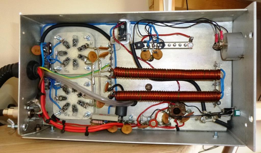
Figure 10 – Heater Choke Arrangement
Commercial amplifiers offer a matched input to accommodate solid state transmitters. A switched Pi or T matching network provides the match. In this case, the exciter is an FT-1000MP containing an auto-tuner. This begs the question: do I really need input tuning? In day-to-day use, the FT-1000MP seems happy enough driving the linear. The auto-tune matches very well.
Without the auto-tuner, the transmitter reports an input VSWR of 2.5 (on 80m) suggesting a load around 125 Ω. An input power of between 40 – 60 Watts seems sufficient to drive the amplifier fully. The corresponding power gain is around 12 dB which is typical for this type of amplifier.
The most difficult part is limiting the FT-1000MP to half-power. The MP ALC circuit is over enthusiastic and creates a huge drive overshoot on the initial syllable of speech. This hopelessly overdrives the amplifier creating splatter. One way of dealing with this is to back off the transmitter IF gain using the FT-1000MP hidden menu option. This reduces the gain, disarms the ALC and reduces the power level to what I want. It generally cleans up the signal. The amplifier does not generate ALC itself.
Cathode Chokes
The cathode choke consisted of two bifilar wound inductors in series. The inductance of each was approximately 50 uH making a total of 100 uH. This may seem rather large, but it was intentional. The lowest frequency is 1.8 MHz at which the impedance of the combined choke is around 1130 Ω inductive. The input impedance of the 813 valves in grounded Grid (GG) is probably 125 Ω resistive. The aim was to minimise the effect of the choke on the input impedance. In retrospect, the second inductor is probably unnecessary. Any residual inductance due to the choke is tuned out by the auto-tuner in any case.
Each cathode choke consisted of 44 bifilar wound turns of 1.5 mm diameter solid copper wire with a total coil length of 144 mm on a 9.7 mm diameter ferrite rod. The ferrite rods were surplus items picked up from a rally and were originally destined for a medium wave radio.
Winding the turns directly onto the rod will cause the ferrite material to break. The best method is to use a wooden spoon handle from the kitchen (10.5 mm diameter in my case). The wire is soft enamelled copper that holds its shape well. A layer of plastic insulating tape on the ferrite rod will stop the rod from rattling and will hold the rod firmly in place. An LCR impedance meter measured the inductance without the ferrite rod at approximately 2.0 uH (measured at 200 kHz). With the ferrite rod inserted, the inductance increased to between 50 uH and 60 uH, which at 1.8 MHz corresponded to a calculated impedance of 565 Ω.
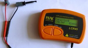
Figure 11 – Peak LCR Meter- Superb
Apart from pliers, cutters and the soldering iron, the most valuable tool in the shack turned out to be a ‘Peak LCR45’ impedance meter that I think is an excellent addition to the shack. This instrument measures the inductance at 200 kHz, but that is fine and provides a very good insight. Using the meter, I could measure RF chokes, tank circuit elements and of course the heater chokes with ease. It also aids with resistor and capacitor markings that are difficult to see at my age. I could check every component including the large electrolytic capacitors in the power supply.
Heater Filter
Balun 3 provides an additional inductance of 5 μH on the heater connection in the form of a Pi-filter. This reduces the egress of conducted emissions out of the PA compartment via the heater wires. In this design, the heater transformer is external and uses long leads making this more important. The common mode choke value is 5 uH formed by winding two bifilar turns on a surplus Manganese Zinc ferrite core. Again, the Peak LCR45 impedance meter came to the rescue providing actual inductor readings in μH and avoided the wild guessing that is so common with home brew.
LTspice provided a useful method to approximate the performance of the filters. Figure 12 shows the input circuit arrangement.
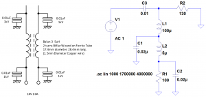
Figure 12 – Heater Common Mode RF Filtering – LTspice Simulation
The choice of the Pi-filter and the larger than normal cathode choke provided a theoretical conducted attenuation of around 60dB at 1.8 MHz. Doubling the size of the heater inductor L1 (in Figure 12) provided an additional 6 dB of attenuation as expected.
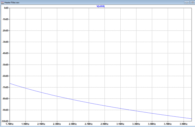
Figure 13 – Heater RF Filtering – Results
Figure 13 shows the results on 160 m and 80 m. It seems to work. The power unit umbilical cord seemed RF dead on all bands.
Heater Voltage
The 813 valve employs a thoriated tungsten filament that operates just below the melting temperature of tungsten at about 2023 K. The delicate filament elements demand respect both physically and electrically. Some texts suggest that turning the heaters on and off can reduce the life of the valve by 0.2% each time. In addition, hard starting the valves increases the transient heater current by a factor of 8.6. In practice, they glow bright at 10 V. If you switch them on hard from cold, they light up like light bulbs! The RCA specification states that the heater voltage must be 10 +/- 5% or in the range 9.5 V to 10.5 V AC.
For this reason, I made the following choices:
1. Soft Start on the power supply including both the EHT and heater supplies.
2. A heater voltage of precisely 10V measured at the valves.
The soft start is just an 88 Ω 400-Watt resistor is series with the AC supply. The resistor consists of four 22 Ω 100-Watt wire wound resistors bolted to the cast aluminium box. Charging of the electrolytic capacitors in the PSU and the heater elements together pull down the applied voltage to the transformers. The effect is that the valves glow slightly but never brightly and the EHT reaches half-voltage approximately. A switch shorts out the resistors when the amplifier is ready for use. An electrical timer could automate this processor. However, a manual switch is more useful. During periods of low-activity, opening the switch renders the power unit and valves in a standby mode. Throwing the switch restores full operation within a few seconds. Figure 4 shows the power arrangements.
With two valves in parallel, the combined heater current is 10 A. The resistance of the heater chokes causes a drop of around 1.4 V. In addition, one leg of the supply passed through a 16 A circuit breaker (mounted on a DIN rail) that dropped 0.85 V. The combined resistance including the heater wires caused a total volt drop of around 2.6 V. A suitable combination of taps on the heater transformer and input mains taps provided a heater voltage of 10.01 V @ 10 A measured on the valve pins.
In many respects, the heater transformer is the most difficult part of the project. It is very difficult to find new (or old) transformers with centre taps rated at 10 V, 10 A. Also, a centre tapped winding is difficult to tap if you need to raise or lower the heater voltage.
Another alternative considered was a 12 V 10 A DC switch-mode power supply but that would involve a lot of engineering to protect the supply and limit the radiated emissions. Switch-mode supply can create receive interference and are best avoided.
Another alternative was to purchase a suitably sized toroidal transformer and unwind the secondary and replace it with 5V – 0 – 5V along with suitable taps. It all seemed like a lot of work but it is probably the best solution in the long run.
Heater Balance
The heater transformer used in this project was an enormous thing with taps ranging from 9 V to 12 V with a floating 0.5 V winding. It was obvious that this would supply far more than 10 A if required. For this reason, the design included a 16 A circuit breaker to avoid unintentional welding. This transformer did not have a centre tap. The question is: how do you connect the valve heaters to HT negative?
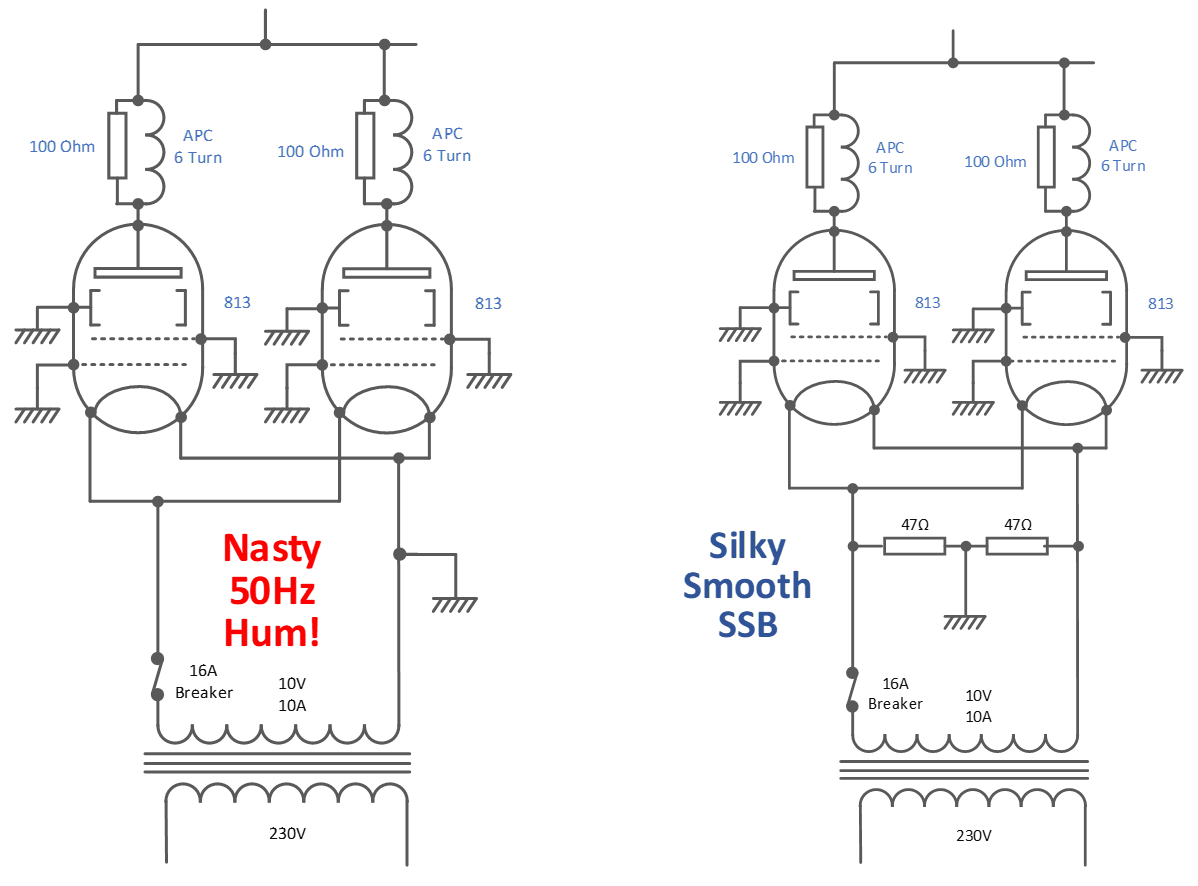
Figure 14 – Cathode Connection
I tried two solutions: The obvious solution is to connect one side of the heater transformer secondary to ground. However, as expected, the transmitted signal contained hum. The other solution is to use two resistors and balance out the hum. In theory, at the peak of the 10 V ac cycle, one side of the heater is at +7.071 V peak (peak value of 5V rms) relative to earth. The other end of the heater is at -7.071 V. The two voltage differences should cancel out. This method worked very well but it did have a slight impact on the DC bias voltage of the two 813 valves.
Figure 14 shows the two solutions diagrammatically. The AC current in the resistor at 50 Hz using two 47 Ω resistors is:
The power in each resistor due to the heater current is:
These resistors also must carry anode current of up to 0.3 A each. Hence, the total current in each resistor is around 0.31 A corresponding to a power of 4.5 W. Two 5 W wire wound resistors sufficed.
The RF drive signal injects directly on the valve heaters at the other end of the heater choke. Hence, the resistors do not influence RF signal performance. However, the DC bias for the valve will pass through the parallel combination creating a bias voltage on the grid that tends to reduce anode current.
In his 1963 article, G2DAF claimed that a single 813 will pass 45 mA with zero grid voltage and zero screen voltage at 2.5 kV anode voltage. Three valves were available for testing. With the valves configured in grounded grid and the bias reduced to zero (two 47 Ω resistors in parallel remained in the cathode circuit), the valve quiescent currents were as follows:
| Valve | HT Voltage | Bias Voltage | Anode Current |
|---|---|---|---|
| Valve 1 | 1800 V | 0 V | 19 mA |
| Valve 1 | 2400 V | 0 V | 27 mA |
| Valve 2 | 2400 V | 0 V | 33 mA |
| Valve 3 | 2400 V | 0 V | 32 mA |
Table 1-Single 813 Quiescent Anode Current Values
In conclusion, V1 seemed a bit weak and was dismissed, but V2 and V3 seem reasonably matched. This table suggested that the two 47 Ω resistors reduced quiescent current possibly by 33% compared with G2DAF’s figures. At 66 mA combined standing current, the grid voltage developed by the resistors is approximately 1.55 V.
Two ways of increasing the quiescent current are:
1. Increase the anode voltage to 3 kV. The quiescent current will increase accordingly.
2. Use a small power supply to force the grid return point negative by a few volts.
The more pragmatic approach is to test the third order IMPs and see if 66 mA is sufficient for linear operation.
Anode Decoupling
It is easy to ignore anode decoupling and make assumptions. However, the HT supply is external and there existed a need to ensure that RF energy did not radiate from the umbilical cable. Two surplus door knob capacitors were available. Each rated at 3.5 kV and labeled as 6,800 pF .
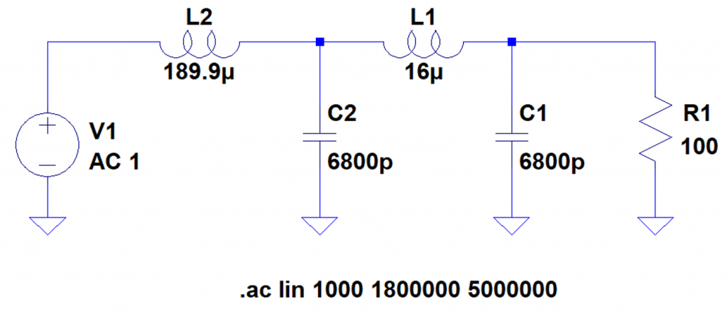
Figure 15 – LTspice Approximation of Decoupling
Rather than paralleling the two together, it is ludicrously easy to incorporate a 16 uH inductor and provide an additional 15 dB attenuation at 1.8 MHz. With the inductor in place, the estimated RF filtering is about -66 dB.
An LTspice simulation of the amplifier on 160 m at 840 W PEP output (See Figure 20) showed that the peak instantaneous voltage across C1 (6800 pF) was virtually the same as the supply rail voltage. A combination of the anode choke and the decoupling capacitors reduced the RF to low levels. For this reason, a voltage rating of 3.5 kV is probably just adequate. Personally, I would prefer more margin.
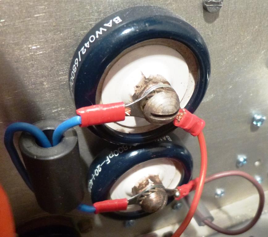
Figure 16 – Anode Filter
The inductor consisted of two turns on a surplus Manganese Zinc core. Again, the Peak LCR45 impedance meter provided quantification at 200 kHz and showed a value of 16 uH. The core and wire must be spaced away from any metal work obviously!
Anode Choke
The anode choke is tricky. My naïve approach was to ensure that the choke provided at least ten times the impedance of the anode load at the lowest usable frequency of the amplifier (1.8 MHz). However, that resulted in an inductance of 521.8 uH – far too big for the higher bands.
I ended up with 105 turns of 0.3 mm diameter copper wire on a 39.6 mm diameter ceramic tube. Spreading the turns evenly over 75 mm gave a measured inductance of 184.5 uH @200 kHz. A superb site for estimating inductance is https://hamwaves.com/inductance/en/index.html. Using the above information, this site estimated the inductance as 185.93 uH @ 2.0 MHz giving a series impedance of approximately 2336.5 Ohms.
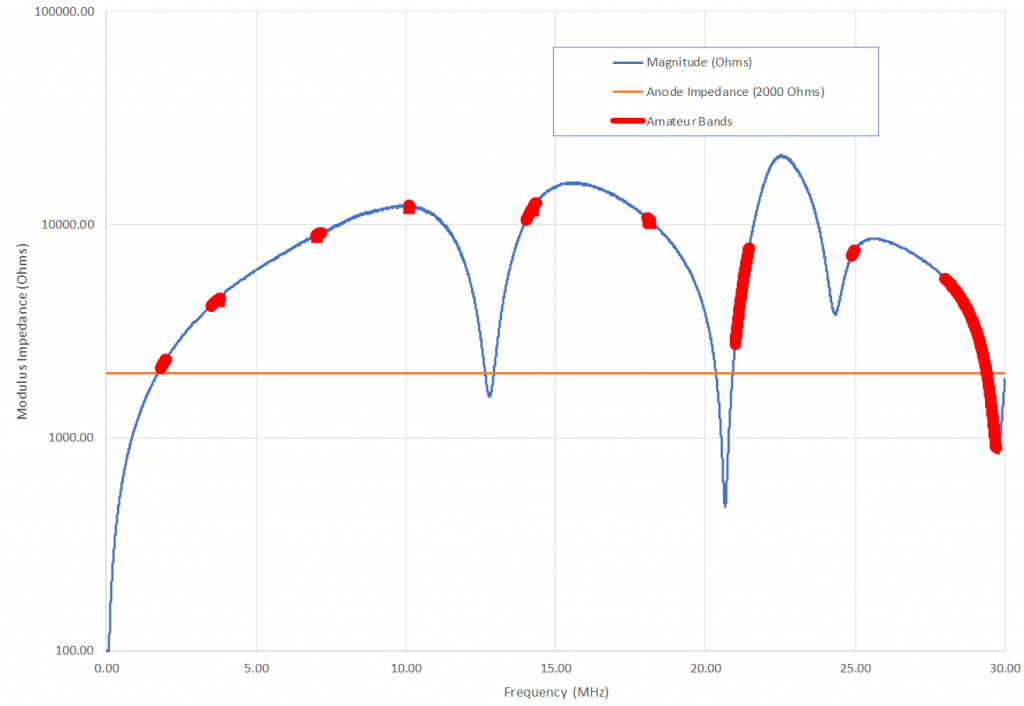
Figure 17 – Impedance Magnitude of the Choke
Figure 17 shows the measured impedance of the choke using a network analyser. The red bars highlight the amateur bands. For this plot, the coil sat on the work bench. Following installation of the choke into the amplifier, the resonances will all change and so the graph is just a rough indication.
In reality, 185.93 μH is too large for the HF bands. Some commercial amplifiers employ two chokes and switch decoupling capacitor to minimise the resonances over the range 2 – 30 MHz. That is a far better solution, but, unfortunately, I do not have spare switch contacts on the band switch. The above graph shows impedance magnitude. At some frequencies, the choke behaves like a high impedance capacitor! despite that, it still works.
Anode Load Impedance
Before calculating the PI-tank components, the first calculation is to determine the optimum load impedance for a given power output. The easy route is to just pick a similar amplifier out of the various handbooks and copy all the tank circuit values blindly. Whilst this works well, nothing is learnt. Learning and understanding must involve pain!
Assuming that the amplifier is 50% efficient and the output power is 700 Watts, then the anode current is approximately 0.6 A at an anode voltage of 2400 V.
The ARRL 1997 handbook suggests the anode load is calculated by:
The ARRL 1983 handbook suggests:
The RSGB Radio Communications Handbook 1969 suggests:
Assuming the peak RF voltage swing is about 80% of Va, giving:
Where do these equations come from? If the amplifier is a push-pull design with ideal valves that pull down all the way from say 2400 V to zero, then the input power developed in the circuit would be simply:
The corresponding anode impedance would be:
This assumes that the voltage and current terms are true RMS quantities and are in phase. For single ended amplifiers, the valves completely cut off during one half of the cycle. Hence, all the work occurs in the other half cycle. For this reason, the anode impedance must be at least half the value shown above in equation 3.
However, the valve cannot pull down all the way to zero volts. Hence, a fudge factor modifies equation 4 to give the correct answer. In Equations 1 and 2, the fudge factor is 1.6 and 1.8 respectively it seems. I chose an output impedance of 3000 Ω. I want to later increase the anode voltage so this value seems appropriate.
Amplifier Spice Evaluation
In this section, I wanted to see if a spice evaluation realistically predicted the output power and intermodulation performance (IMP) of an 813 linear. Audio enthusiast routinely simulate valve amplifier circuits using LTspice. I ‘doff my hat’. I have never seen this done on valve RF amplifiers before so this was moderately exciting.
Using an anode load impedance of 3000 Ω, and the PI-tank values calculated in this document, I created an LT-spice simulation to see what happens. I found a spice file called ‘tetrode.txt’ described in an audio blog that contained a definition for the 813.
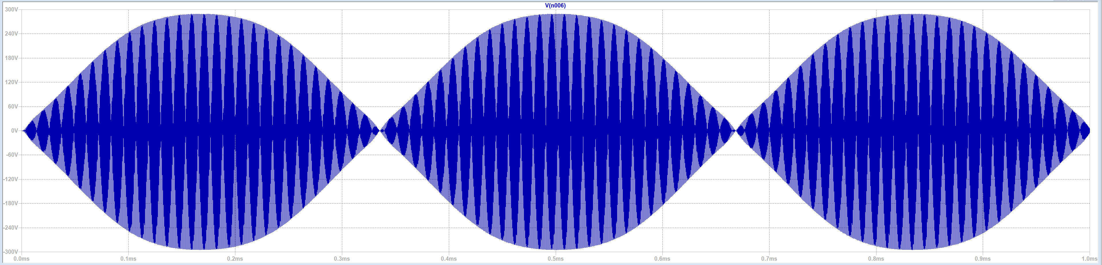
Figure 19 – LTspice Simulated RF Output Envelope on 160m at 780 Watts PEP Output
To be thorough, I compared the anode curves against those depicted in the original 1955 RCA specification. The curves were surprisingly close. Changing some of the spice parameters corrected the model so that it matched the RCA figures almost exactly.
I tried both models in the amplifier simulation and found the results very similar. For that reason, I decide to use the original model. In any case, the parameters of the 813 will probably vary from valve to valve and these may depend upon the exact voltage applied to the heaters. The model appeared close enough to the RCA manufactures figures to attempt a meaningful simulation.
The results were almost exactly as expected. With a 3000 Ω anode load, the output two-tone RF envelope measured at the 50 Ω load started to flat-top at about the 900 Watts level. Figure 19 shows the output load waveform at 780 Watts PEP. It was necessary to reduce the PI-tank C8 capacitor slightly (See Figure 20) to accommodate the anode to cathode capacitance built into the spice model. This modification ensured correct tuning and impedance transformation at the resonance frequency of 1.9 MHz. An LTspice frequency scan ensured that the PI-tank did indeed resonate at 1.9 MHz. LT-Spice is very powerful.
Just as a note, the licenced UK power at 1.9 MHz is 15 dBW or 31.6 Watts output and not 780 Watts. However, it is easier to run LT-spice on the lowest band and at the frequency used to calculate the PI-Tank components. There is no intention to operate the amplifier for real at this frequency! Honestly!
The simulation in Figure 20 employed two 813 valves in parallel connected in grounded grid and included an anode choke, decoupling capacitors and the power filter. Rf drive to the cathode consisted of two 70 V peak sources: one at 1.9 MHz and the other at 1.903 MHz separated by 3 kHz.
The simulation used 1 ns steps over 1 ms to ensure the capture of three complete cycles of the two-tone modulation. This provided a clean Fourier transform of the output allowing visualisation of the estimated third order intermodulation products (IMPs). The 22 Ω resistor R5 represents the heater resistors in parallel. The anode current must pass through these but they are decoupled by capacitors C4 and C5. LTspice reported the ambient anode current as 61 mA.
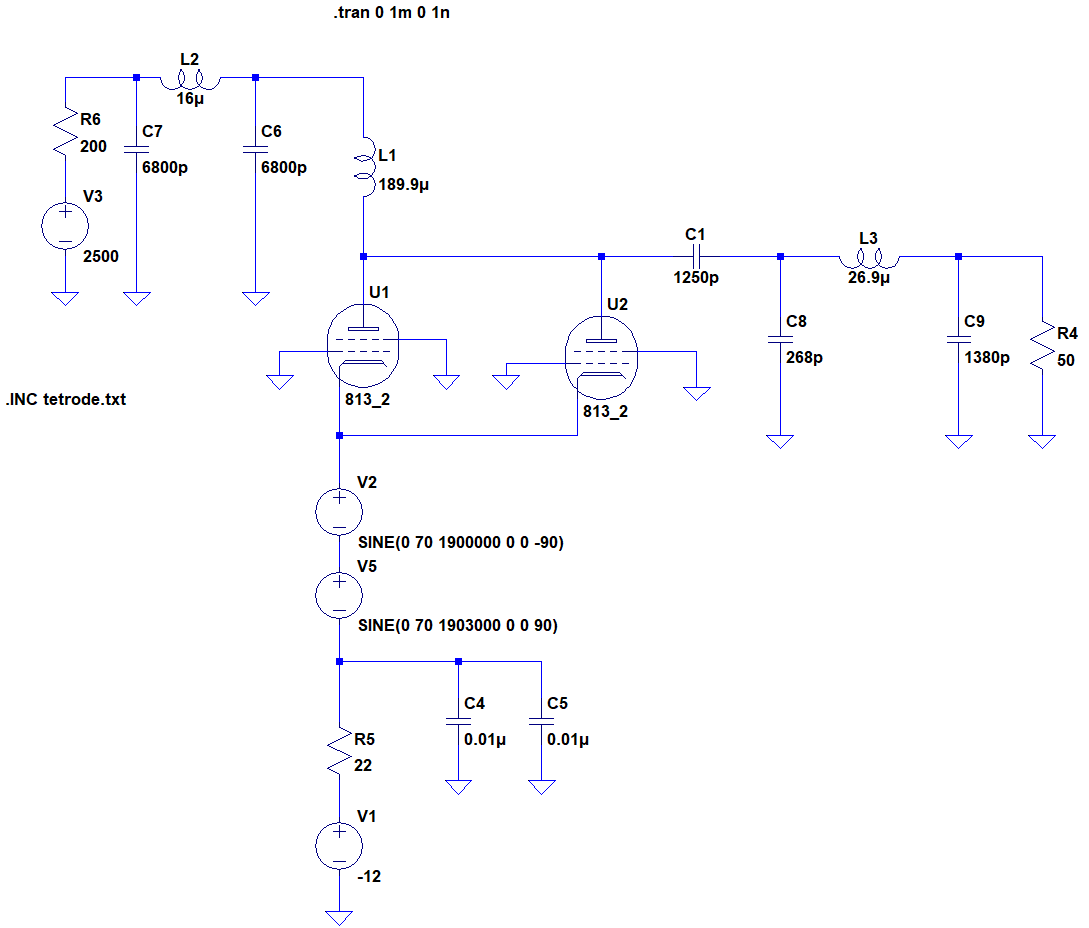
Figure 20 – LTspice Simulation – 160 m – 780 Watts PEP Output
The simulation is a rough estimate. However, is does allow the experimenter to mess about with components and drive levels to optimise elements of the design without killing oneself by sticking probes into high voltage circuits. Circuit simulation permits resolution of issues and problems during the design stage making any actual tests on the RF deck virtually obsolete.
As a general note, I resist from performing any measurement on live circuits containing exposed EHT – it is just not clever. At some stage, even with great care and experience, it is inevitably that a hand or finger may accidentally touch an exposed circuit and ZAP – ‘that is that’ – a quick route to the wooden box.
For this simulation, the peak RF drive voltage was 140 V on the cathode. Assuming a drive impedance of around 125 – 150 Ω, then the drive power is around 60 – 70 Watts peak envelope power (PEP). The corresponding amplifier gain is about 10 – 11 dB. These figures fall within expected values and are almost believable.
Figure 21 shows the anode waveform in black, the drive waveform on the cathode in blue and the HT volts in red. At any time, the minimum voltage across the anode and cathode of the 813 valves is 260 V during peak conduction.
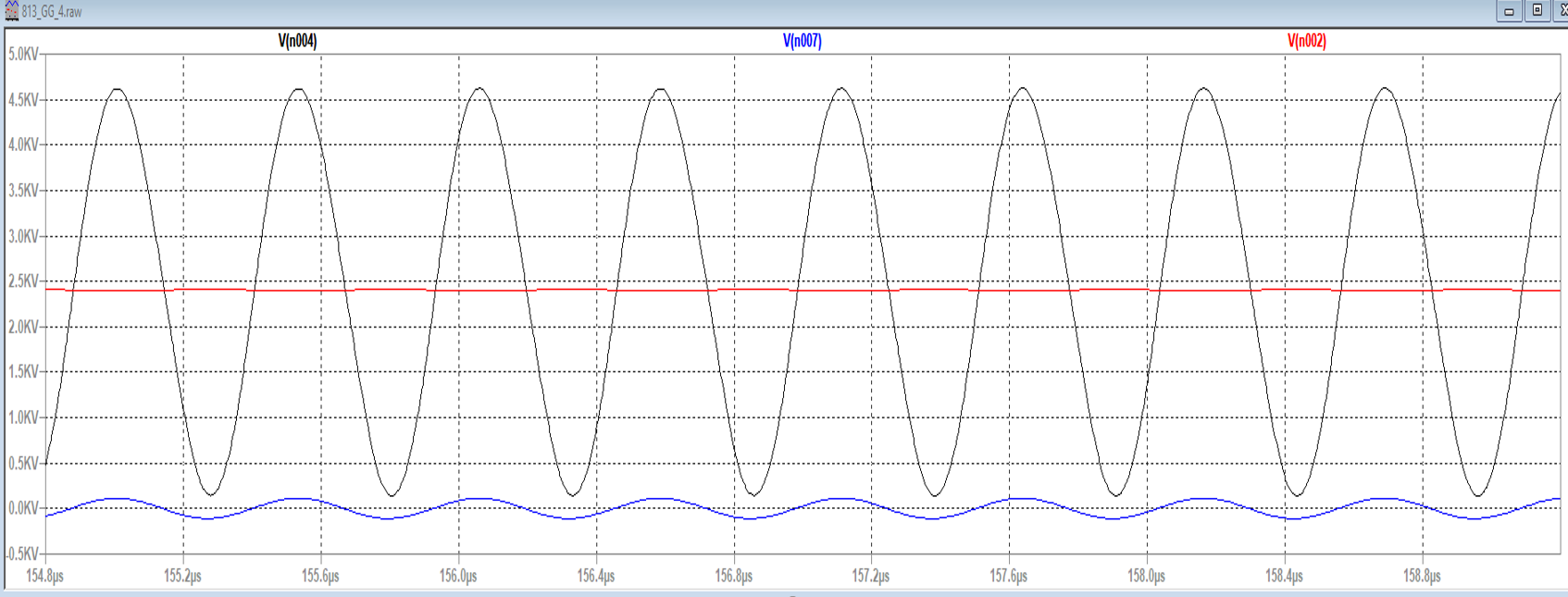
Figure 21 – Anode Waveform
The maximum voltage on the anode is around 4.5 kV and so the decoupling capacitor feeding the PI-tank must be substantial. The one used in this design is 1250 pF rated at 10 kV. I have to admit, the choice of 10 kV for the decoupling capacitor was accidental – one just happened to be available. I had completely forgotten that the peak voltages in the anode circuit adds to the anode supply and can reach very high levels typically 5 kV or more. The LT-spice simulation proved a good reminder. I wonder how many amplifiers contain underrated capacitors?
Please note: the 813 valve is directly heated without a cathode. However, it is easier to refer to the cathode rather than confuse the issue by referring to the heater.
Figure 22 shows the LTspice simulated output inter-modulation products (IMP) at a level of -36 dB on either tone. That suggests a figure of 42 dB below PEP. If this is correct and if it translates into reality, the amplifier will probably be better than the FT-1000MP driver.
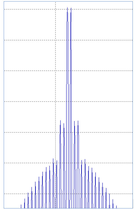
Figure 22 – Simulated Output IMP of the Amplifier – 160 m @ 780 Watts PEP
Reducing the ambient current from 61 mA to 51 mA drops the IMPs to -30 dB on either tone. It seems that 61 mA may be the minimum acceptable value. A figure of 80 mA standing current is probably a better value.
The LT-spice model allows the experimenter to estimate the third order IMPs at different power levels. These were all calculated at 1.9 MHz using the PI-Tank values calculated later in this document.
| Drive voltage (V) (Each tone Peak) | PEP Output (Watts) | 3rd order IMP relative to each tone (dB) | IMP relative to PEP (dB) |
|---|---|---|---|
| 70 V | 780 W | 36.0 dB | 42.0 dB |
| 40 V | 492 W | 38.7 dB | 44.8 dB |
| 30 V | 267 W | 41.0 dB | 47.0 dB |
| 20 V | 113 W | 35.1 dB | 41.1 dB |
| 10 V | 30 W | 26.5 dB | 32.5 dB |
Table 2 – Estimated 3rd Order IMP
Original 813 Spice File (Audio Blogger) – Close Fit to RCA 1955 Anode Curves
.SUBCKT 813 1 4 2 3
+ PARAMS: MU=8.5 EX=1.414 KG1=2720 KP=46.2 KVB=132
+         CCG=16.3P CPG1=.25P CCP=14P RGI=3.3K
RE1  7 0  1MEG    ; DUMMY SO NODE 7 HAS 2 CONNECTIONS
E1   7 0  VALUE=  ; E1 BREAKS UP LONG EQUATION FOR G1.
+{V(4,3)/KP*LOG(1+EXP((1/MU+V(2,3)/V(4,3))*KP))}
G1   1 3  VALUE={(PWR(V(7),EX)+PWRS(V(7),EX))/KG1*ATAN(V(1,3)/KVB)}
* G2     4 3  VALUE={(EXP(EX*(LOG((V(4,3)/MU)+V(2,3)))))/KG2}
g2   4 3  value= {(I(G1)*50/(V(1,3) + 2))} ; models change in current with change in plate
RCP  1 3  1G      ; FOR CONVERGENCE
C1   2 3  {CCG}   ; CATHODE-GRID 1
C2   1 2  {CPG1}  ; GRID 1-PLATE
C3   1 3  {CCP}   ; CATHODE-PLATE
R1   2 5  {RGI}   ; FOR GRID CURRENT
D3   5 3  DX      ; FOR GRID CURRENT
.MODEL DX D(IS=1N RS=1 CJO=10PF TT=1N)
.ENDS
Modified 813 Parameters – Very Close Fit to the RCA 1955 Document
.SUBCKT 813 1 4 2 3
+ PARAMS: MU=8.5 EX=1.414 KG1=3500 KP=46.2 KVB=70
+         CCG=16.3P CPG1=.25P CCP=14P RGI=3.3K
RE1  7 0  1MEG    ; DUMMY SO NODE 7 HAS 2 CONNECTIONS
E1   7 0  VALUE=  ; E1 BREAKS UP LONG EQUATION FOR G1.
+{V(4,3)/KP*LOG(1+EXP((1/MU+V(2,3)/V(4,3))*KP))}
G1   1 3  VALUE={(PWR(V(7),EX)+PWRS(V(7),EX))/KG1*ATAN(V(1,3)/KVB)}
* G2     4 3  VALUE={(EXP(EX*(LOG((V(4,3)/MU)+V(2,3)))))/KG2}
g2   4 3  value= {(I(G1)*50/(V(1,3) + 2))} ; models change in current with change in plate
RCP  1 3  1G      ; FOR CONVERGENCE
C1   2 3  {CCG}   ; CATHODE-GRID 1
C2   1 2  {CPG1}  ; GRID 1-PLATE
C3   1 3  {CCP}   ; CATHODE-PLATE
R1   2 5  {RGI}   ; FOR GRID CURRENT
D3   5 3  DX      ; FOR GRID CURRENT
.MODEL DX D(IS=1N RS=1 CJO=10PF TT=1N)
.ENDS
The above table is a copy of the two spice models used as sub-circuits in LTspice. The first file originates from audio blogs. The second table is the modified version. Figure 23 shows the actual circuit simulated. The inter-electrode capacitance values are identical to those in the 1955 RCA 813 specification (page 3).
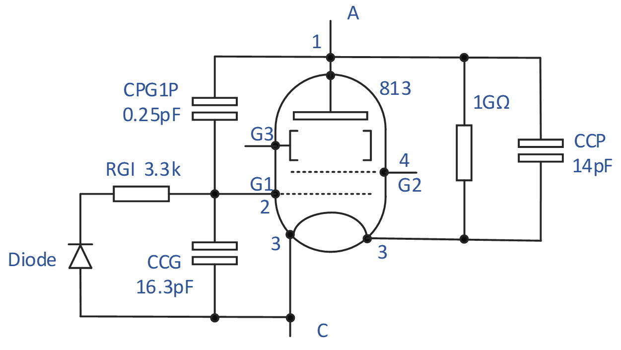
Figure 23 – Spice Representation
In normal maths notation, the equation in the modified spice models is as shown below.
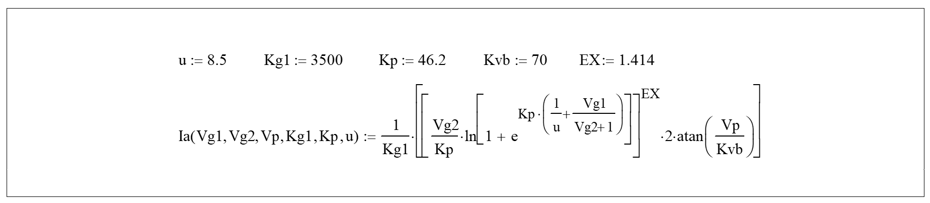
Figure 24 – Spice Parameters for a single 813
The appendix in this document illustrates a comparison between plots of anode characteristics provided by the 1955 RCA 813 specification and those generated by the modified LTspice model.
PI-Tank Components
From previous discussions, a load impedance of 3000 Ω seems a logical choice. The next stage is to calculated the PI-tank components. In another document, I spent days working out equations for PI-tank circuits. These calculations assumed a working Q and knowledge of the input and output impedance. The following equations are the results:
PI-tank Calculations: Here, R=50Ω, Rp=3000Ω and Q is the loaded Q factor of the PI-Tank with R connected.
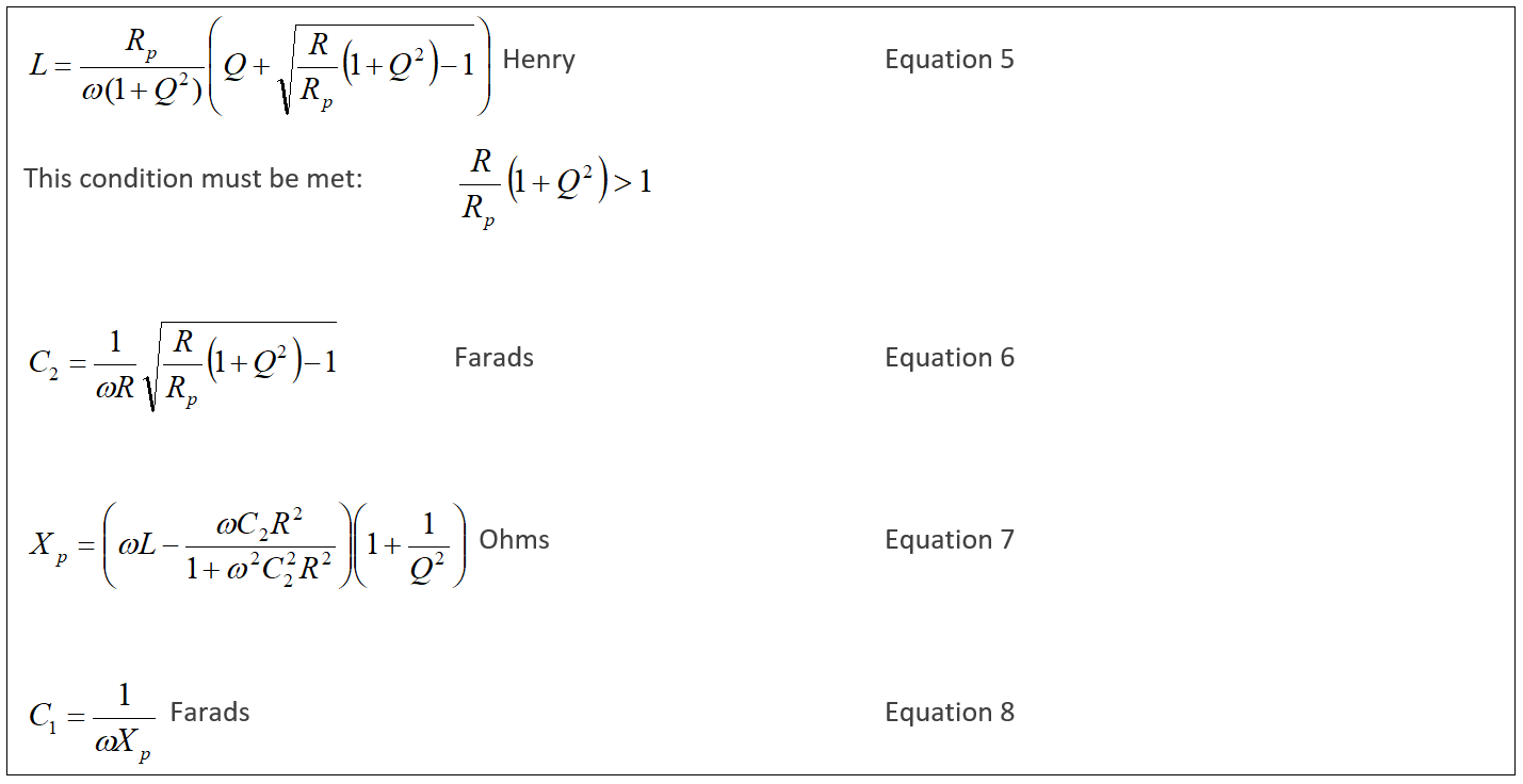
It is best to work them out in the order shown.
As it happens, these equations are essentially identical to those in the “Eimac Care and Feeding of Power Grid Tubes” book. The site: https://owenduffy.net/calc/pi.htm describes a calculator based on the Eimac equations that gives identical results. This makes it very easy to calculate components. Note that equation 5 looks different to the corresponding equation in the Eimac publication but both forms give exactly the same results. The two equations are, in fact, equivalent.
The linear employs a 28 – 500 pF variable vacuum capacitor for C1 and a 1500 pF variable capacitor for C2. Any tank circuit solution must fall within these capacitor ranges otherwise switching becomes necessary.
On 10 m and 15 m, raising the Q is advantageous. This makes the required value of C1 larger. The hope is that the anode capacitance and circuit strays in parallel with C1 remains low enough to enable correct tuning.
The stray capacitance of the tank circuit with no valves but including the minimum capacitance of C1 is approximately 28 pF. Each valve introduces another 14 pF so the total anode capacitance is around 56 pF. That is high and is one of the main disadvantages of using the 813 valve on 15 m and 10 m.
Table 4 – PI-Tank Values
| Bands | C1 | C2 | L | Q |
|---|---|---|---|---|
| 1.9 MHz | 279 pF | 1380 pF | 26.9 uH | 10 |
| 3.7 MHz | 186 pF | 1160 pF | 10.9 uH | 13 |
| 7.1 MHz | 97.1 pF | 607 pF | 5.68 uH | 13 |
| 14.2 MHz | 48 pF | 304 pF | 2.84 uH | 13 |
| 21.2 MHz | 32.5 pf | 203 pF | 1.90 uH | 13 |
| 28.2 MHz | 30.1pF | 188 pF | 1.17 uH | 16 |
It is obvious from the above table that 14, 21, and 28 MHz will not tune due to C1. In practice, 14 MHz just squeezed in but with the vacuum capacitor almost fully extracted. It was necessary to move the coil tap and raise the Q on this band to allow sensible tuning. I abandoned 18, 21, 24, and 28 MHz as a lost cause. To cover these bands, C1 would need replacing with smaller values and band switches to cover the range. Another alternative is to place a smaller capacitor in series with C1 but switch it out on the lower bands.
The LCR meter helped when choosing taps on the tank coil for each band. I chose taps as close as possible to the values shown in Table 4. The measured inductance usually fell above or below the wanted value. Inevitably, some fiddling around is necessary.
The next part looks into covering WARC bands. However, this is now largely academic apart from 10 MHz band. The enormous ceramic band switch used in the tank circuit had only 6 positions! I originally intended to cover the WARC bands using the existing positions. Armed with Equations 5 to 9, it is possible to determine the performance. Rearranging equation 5 allows calculation of Q for a fixed L. The value of ‘L’ is value in the table above.
Rearranging Equation 5:
This rearrangement is quite tricky to perform. Q ends up as a quadratic equation with two solutions. The above is always the correct version. I have derived this in another document.
Table 5 – WARC Bands
| WARC Band | Adopted Band | Fixed L | C1 | C2 | Q |
|---|---|---|---|---|---|
| 10.1 MHz | 7.1 MHz | 5.68 uH | 45.8 pF | 167.0 pF | 8.7 |
| 14.2 MHz | 2.84 uH | 97.4 pF | 686.9 pF | 18.5 | |
| 18.1 MHz | 14.2 MHz | 2.84 uH | 29.1 pF | 142.6 pF | 9.9 |
| 21.2 MHz | 1.90 uH | 45.0 pF | 302.0 pF | 15.4 | |
| 24.9 MHz | 21.2 MHz | 1.90 uH | 23.3 pF | 128.3 pF | 10.9 |
| 28.2 MHz | 1.17 uH | 38.9 pF | 273 pF | 18.3 |
Two options exist for each WARC band.
For 10 MHz use 14 MHz band Q=18.5
For 18 MHz use 21 MHz band Q=15.4
For 24 MHz use 28 MHz band Q=18.3
The 10 MHz solutions tunes with C1 =97.4 pF but all the other solutions fail. The best overall solution is to buy a properly designed commercial amplifier that works well!
A Quiet Fan
This sounds obvious but it is important. The fan must be whisper quiet. I find it amazing that some amateurs, when requiring a cooling fan, go to the nearest rally and buy a buggered up 230 V thing with worn bearings for a few pence and then wonder why it is noisy. The fan used in this design is a 100mm diameter 12 Volt computer fan with a noise level claimed to be 13 dBA at 1 metre. It is so quiet that I cannot hear it at all when the amplifier is in position in the shack. I also have the option of engaging the built-in blue and red flashing LEDs. Generally, the larger the diameter of the fan the better.
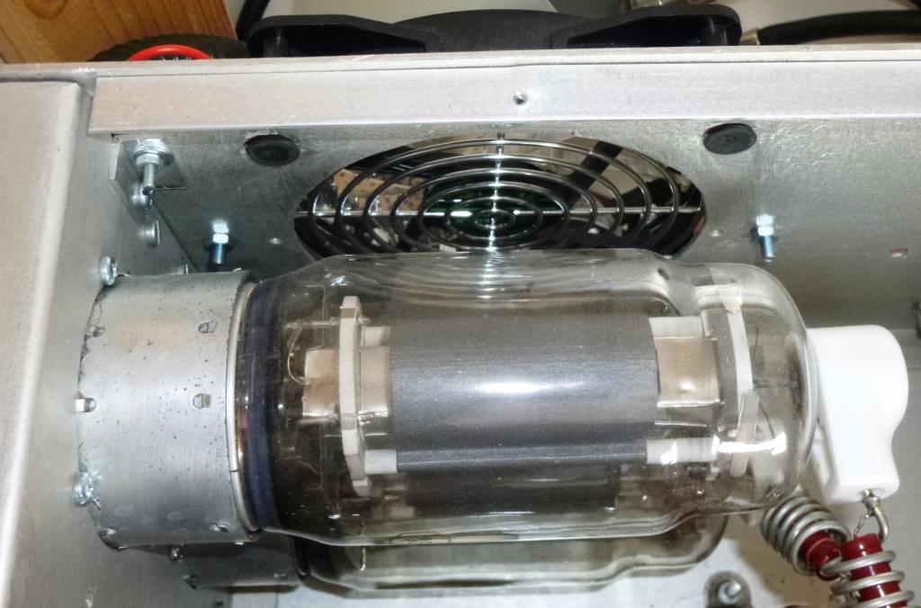
Figure 25 – Fan Grill – Keeps Fingers and RF Out
To maintain silence, I cut a hole 100mm diameter in the rear panel immediately behind the 813 valves. I used a metal fan grill that bolts directly to the panel. This maintains the shielding of the valve compartment but impeded the air flow only slightly. The fan itself mounts on four rubber bungs. The bungs push into holes in the chassis and the fan fixings screw into the rubber. The air flowing into the valve compartment falls directly onto the glass envelopes.
Air flow for the 813 is not critical at all. However, I mount my valves horizontal one above the other (which is awful really). It suggests that the upper valve will receive the rising heat from the other. A steady air flow keeps the heat moving. When mounting the 813s horizontal, align the grids vertical to stop them sagging.
Conclusions
I have not yet measured the IMPs of the amplifier. It is quit difficult to do it properly. I could measure the IMPs of the exciter at the input and then measure the IMPs at the output. Ideally I need a hybrid transformer and two 10 – 70 Watts independent transmitters and a tuning unit to test it properly. I will update this site once it is done if I can do it. Reports on the air are complementary and observation on an SDR band scope show a narrow and contained signal. I conclude that it cannot be that bad.
Output power is as expected. A single tone output of 800 W is easy to achieve on all the bands that tune. At 800 W, the valve anodes start glowing red and so this level of power is not sustainable. A pair of 813s should not really be used much above 400 W output. The efficiency is around 50-60%.
The amplifier gain is much higher on 7.0 MHz for some reason. The input bifilar wound heater chokes could resonate making the amplifier more frisky. I wonder if the second heater choke is responsible for that.
I am impressed with LTspice. The simulations appear to be close to the truth and useful. In fact, I may not bother measuring the IMPs of the amplifier and assume the results fall in line with the simulation. On air reports support this approach.
Finally, I was amazed that the PI-tank calculations worked and predicted tuning issues before switching on. If this amplifier was properly designed from scratch, all the tuning issues and difficulties could be avoided. I would not use the 813 in a new design!
Appendix 1
This appendix outlines a comparison between anode curves generated by a LTspice model for the 813 valve and data supplied in a commercial 1955 RCA specification. For these tests, the configuration for a single 813 is common cathode with either 300 or 400 V applied to the screen grid. RCA connect the beam connection to the heater centre tap.
The LTspice model uses the same arrangement and increments the control grid VG1 in 20 V steps from -20 V to 100 V. For each VG1 step, LTspice calculates the anode current for a given anode voltage. In the graphs below, the dots represent data from the RCA document. The RCA data, taken from the data sheet, required rulers, pens, patience and a magnifying glass. The following Mathcad sheet makes the comparison easy.
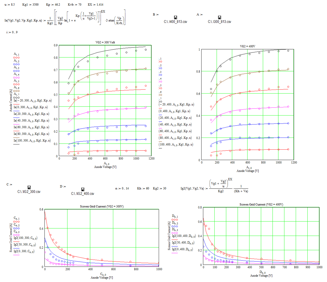
Figure 26 – Comparison of Measured and Estimated 813 Anode Characteristics
The data fit is quite good. RCA probably faced accuracy limitations when they originally recorded the data. Inevitably, differences will exist between different valves, between each tests and results will depend on the accuracy of the heater voltage and screen grid voltage.
73 Chris